(Seoul=Yonhap Infomax) Hak Seong Kim – Applied Materials Inc., a leading global semiconductor equipment manufacturer, has introduced three new technologies aimed at accelerating innovation in logic and memory chips.
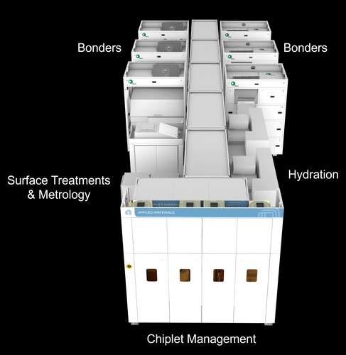
Of particular note, Applied Materials unveiled a product that integrates the hybrid bonding process—considered a next-generation chip stacking technology—into a single system. The company emphasized its contribution to the development of advanced semiconductors, including high bandwidth memory (HBM).
On the 26th, Applied Materials held a press conference at a hotel in Gangnam-gu, Seoul, to introduce the Kinex Bonding System, Centura Extera Epi System, and Provision 10.
Advanced packaging technologies that combine multiple chiplets into a single unit are drawing attention as a way to enhance semiconductor performance and power efficiency. Effective packaging is also critical in HBM manufacturing.
The newly unveiled Kinex system integrates multiple steps required for hybrid bonding—a next-generation packaging technology—into a single piece of equipment. Currently, HBM stacking involves creating bumps between DRAM chips and bonding them using heat and pressure. In contrast, hybrid bonding directly connects chip surfaces without bumps, improving both performance and thermal efficiency compared to conventional methods.
An Applied Materials representative stated, "As packaging becomes more complex, hybrid bonding is an essential technology," adding, "All three major HBM manufacturers—Samsung Electronics Co., Ltd., SK hynix Inc., and Micron Technology, Inc.—are developing this technology."
Applied Materials collaborated with Dutch equipment maker BESI to streamline the complex bonding process into a single workflow. As a result, the process time has been reduced from 13 hours to just one hour, significantly lowering operational risks for semiconductor fabs, the company highlighted.
The Extera system, also introduced at the event, is a deposition tool designed to maximize precision. It is used to implement gate-all-around (GAA) transistor structures in advanced processes below 2 nanometers (nm).
The Provision 10 metrology system improves nanoscale image resolution by 50% and imaging speed by tenfold compared to previous technologies. It is an essential tool for sub-2nm logic and HBM manufacturing processes.
Applied Materials stated that numerous global customers in logic, memory, and back-end processes are already utilizing the newly introduced equipment.
Park Kwang Sun, President of Applied Materials Korea, commented, "Memory plays a pivotal role in artificial intelligence (AI)," adding, "2026 will be a year of significant growth for Applied Materials."
Applied Materials Inc., headquartered in the United States, is a manufacturer of semiconductor and display equipment. In the fiscal year ended last month, the company posted record annual revenue of $28.4 billion (approximately 41 trillion won).
hskim@yna.co.kr
(End)
Copyright © Yonhap Infomax Unauthorized reproduction and redistribution prohibited.